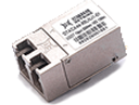
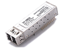
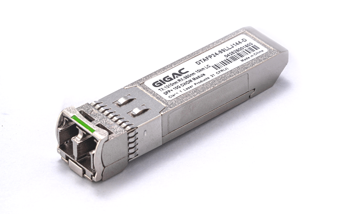
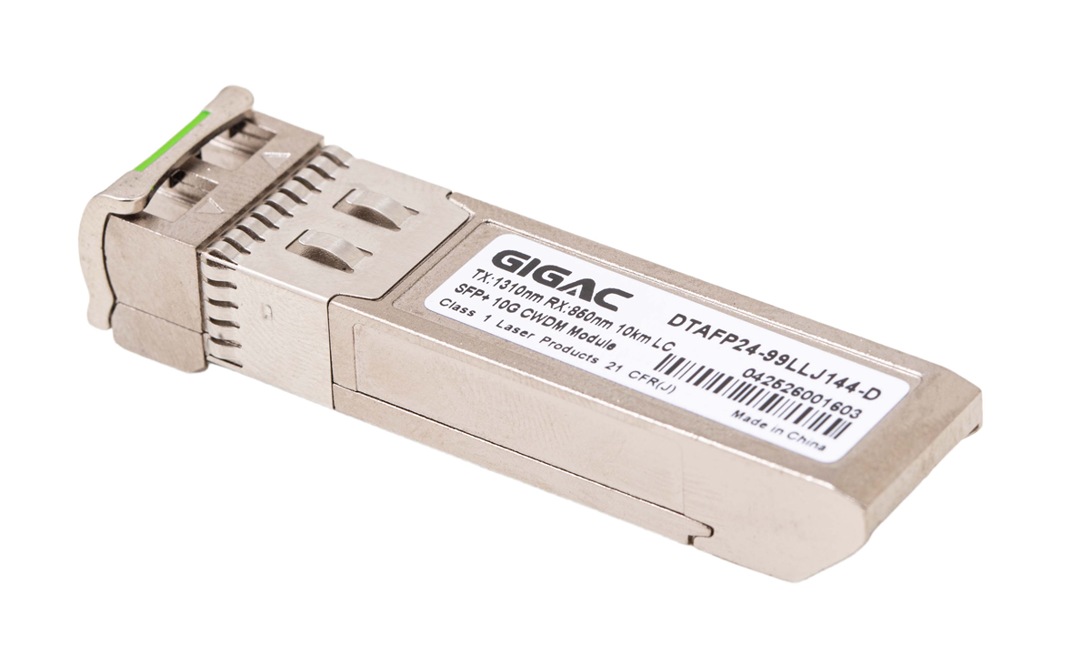
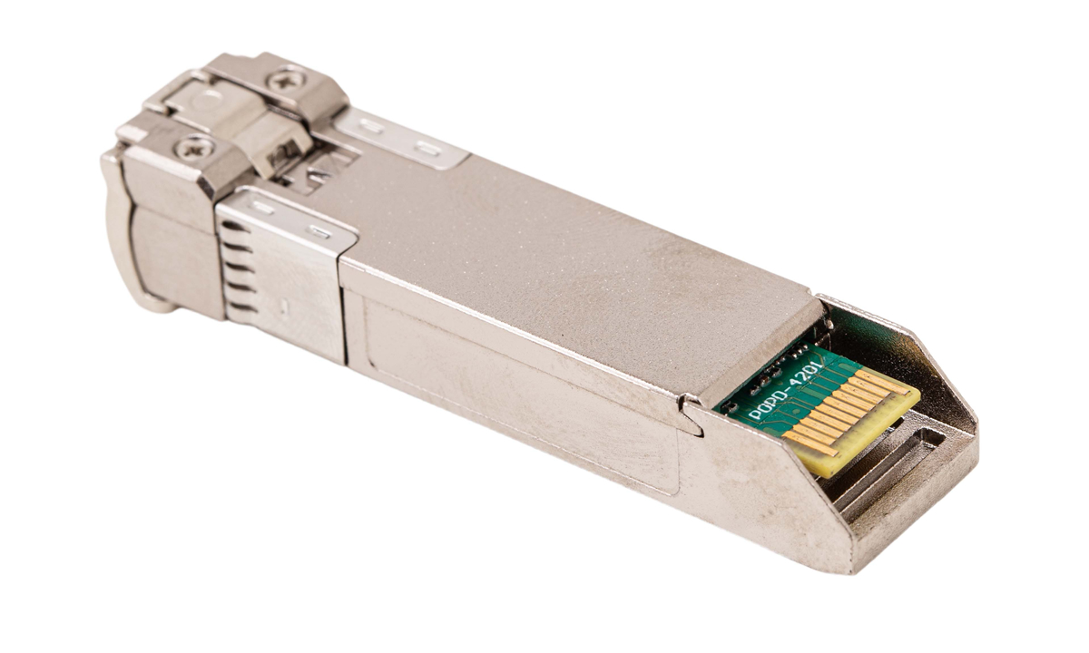
The GACC-3512/5312-10D CSFP transceivers are compatible with the Compact Small Form- Factor Pluggable (CSFP) Multi-Source Agreement (MSA) option 2, The transceiver consists of 2-channel Bi-directional Optical Transceiver unit with five sections: the LD driver, the limiting amplifier, the digital diagnostic monitor, the 1310nm FP laser (the 1550nm DFB laser) and the PIN photo-detector .The module data link up to 10KM in 9/125um single mode fiber.
The optical output can be disabled by a TTL logic high-level input of Tx Disable, and the system also can disable the module via I2C. Tx Fault is provided to indicate that degradation of the laser. Loss of signal (LOS) output is provided to indicate the loss of an input optical signal of receiver or the link status with partner. The system can also get the LOS (or Link)/Disable/Fault information via I2C register access.
Conventional SFP will function when plugged into a C-SFP socket, at the same time no damage to C-SFP and host board if C-SFP module is plugged into a conventional SFP socket
Features
1250Mbps Typical Data Rate and compliant to 1000Base BX10 IEEE802.3ah
1310nm FP laser transmitter for GACC-3512-10D
1550nm DFB laser transmitter for GACC-5312-10D
PIN photo-detector
Ultra-Low consumption
Up to 10km on 9/125µm SMF
Hot-pluggable CSFP footprint
LC/UPC type pluggable optical interface
Achieve operational compatibility with conventional SFP
Metal enclosure, for lower EMI
RoHS compliant and lead-free
Single +3.3V power supply
Support Digital Diagnostic Monitoring interface
Compliant with SFF-8472
Case operating temperature: Industrial / Commercial optional, 0°C to +70°C
Applications
Gigabit Ethernet(1000BASE-BX10)
Point to Point FTTH Application
Switched Backplane Applications
Router/Server Interface
Switch to Switch Interface
Pin Descriptions
Pin | Name | Function | Notes |
1 | VEE | Transceiver Ground | VEE may be internally connected within the SFP module |
2 | TX FAULT | Transmitter Fault Indication | TX Fault is an open collector/drain output, which should be pulled up with a 4.7K–10K resistor on the host board. Note 1 for more information |
3 | TX1_ Disable | Transmitter Disable of Ch A | Module channel A disables function |
4 | MOD-DEF2 | Two-wires interface Data | 2 wire serial ID interface, SDA |
5 | MOD-DEF1 | Two-wires interface Clock | 2 wire serial ID interface, SCL |
6 | TD2- | Inverted Transmit Data Input of Ch B | These are the differential transmitter puts. They are AC-coupled, differential lines with 100 differential termination inside the module. The AC coupling is done inside the module and is thus not required on the host board |
7 | TD2+ | Transmit Data Input of Ch B | |
8 | LOS1 | Loss of Signal of Ch A | Loss of Signal detected function. Note 2 for more information. |
9 | RD2+ | Received Data Output of Ch B | These are the differential receiver outputs. They are AC coupled 100 differential lines which should be terminated with 100(differential) at the user SERDES. The AC coupling is done inside the module and is thus not required on the host board. |
10 | RD2- | Inverted Received Data Output of Ch B | |
11 | VEE | Transceiver Ground | VEE may be internally connected within the SFP module. |
12 | RD1- | Inverted Received Data Output of Ch A | These are the differential receiver outputs. They are AC coupled 100 differential lines which should be terminated with 100(differential) at the user SERDES. The AC coupling is done inside the module and is thus not required on the host board. |
13 | RD1+ | Received Data Output of Ch A | |
14 | LOS2 | Loss of Signal of CH B | Loss of Signal detected function. Note 2 for more information. |
15 | VCCR | Receiver Power | 3.3V± 5%. Note 3 for more information |
16 | VCCT | Transmitter Power | 3.3V± 5%. Note 3 for more information |
17 | TX2_ Disable | Transmitter Disable of Ch B | Module channel B disables function |
18 | TD1+ | Transmit Data Input of Ch A | These are the differential transmitter puts. They are AC-coupled, differential lines with 100 differential termination inside the module. The AC coupling is done inside the module and is thus not required on the host board |
19 | TD1- | Inverted Transmit Data Input of Ch A | |
20 | VEE | Transceiver Ground | VEE may be internally connected within the SFP module. |
Note 1: When high, output indicates a laser fault of some kind either in Channel A or Channel B. The Host shall read Channel A/B for details: TX Fault from channel A if bit 2 is set in [A2H:110]; TX Fault from channel B if bit 2 is set in [B2H: 110]. Low indicates normal operation. In the low state, the output will be pulled to < 0.8V.
Note 2: When high, this output indicates the received optical power is below the worst-case receiver sensitivity (as defined by the standard in use). Low indicates normal operation. In the low state, the output will be pulled
to < 0.4V.
Note 3: VccT VccR are the power supplies. They are defined as 3.3V ±5% at the SFP connector pin. Maximum supply current is 400Ma@3.3V. Vcc may be internally connected within the SFP transceiver module.
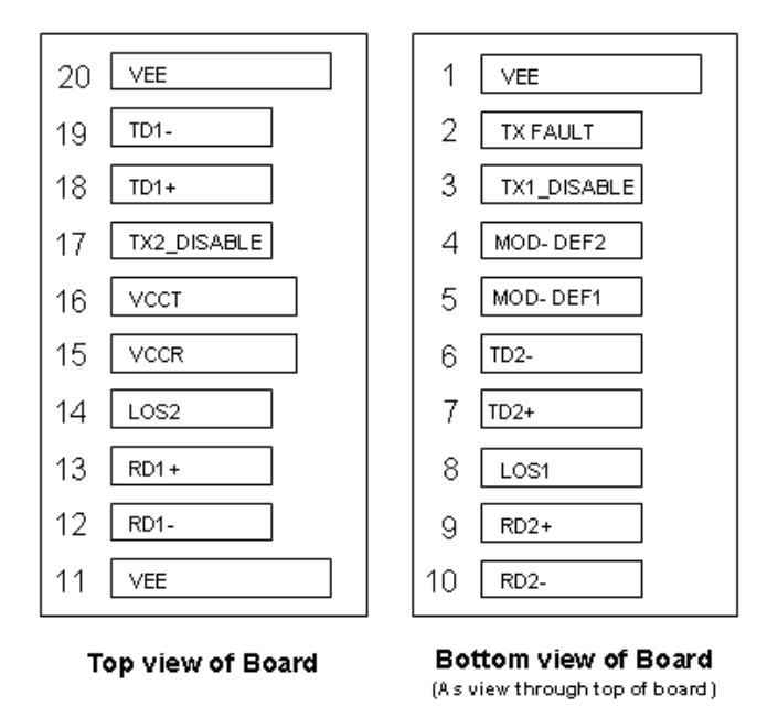
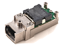
Figure 2: Pin out of Connector Block on Host Board
Absolute Maximum Ratings
Parameter | Symbol | Min. | Typ. | Max. | Unit | Note |
Storage Temperature | Ts | -40 | 85 | ºC | ||
Relative Humidity | RH | 5 | 95 | % | ||
Power Supply Voltage | VCC | -0.5 | 4 | V | ||
Signal Input Voltage | -0.3 | Vcc+0.3 | V | |||
Receiver Damage Threshold | 3 | dBm |
Recommended Operating Conditions
Parameter | Symbol | Min. | Typ. | Max. | Unit | Note | |
Case Operating Temperature | Tcase | 0 | 70 | ºC | |||
Power Supply Voltage | VCC | 3.15 | 3.3 | 3.45 | V | ||
Power Supply Current | ICC | 160 | mA | @25℃(case) | |||
180 | @70℃(case) | ||||||
Power Supply Noise Rejection | 100 | mVp-p | 100Hz to 1MHz | ||||
Data Rate | 1.25/1.25 | Gbps | TX Rate/RX Rate | ||||
Transmission Distance | 10 | KM | |||||
Coupled Fiber | Single mode fiber | 9/125um SMF | |||||
Specification of Transmitter
Parameter | Symbol | Min. | Typ. | Max. | Unit | Note |
Average Output Power | POUT | -15 | -3 | dBm | Note (1) | |
Extinction Ratio | ER | 8 | dB | |||
Center Wavelength | λC | 1260 | 1310 | 1360 | nm | GACC-3512-10D |
1500 | 1550 | 1600 | GACC-5312-10D | |||
Spectrum Width (RMS) | σ | 3.5 | nm | FP Laser (TX:1310nm) | ||
Side Mode Suppression Ratio | SMSR | 30 | dB | DFB Laser (TX:1550nm) | ||
Spectrum Bandwidth(-20dB) | σ | 1 | nm | |||
Transmitter OFF Output Power | POff | -45 | dBm | |||
Differential Line Input Impedance | RIN | 90 | 100 | 110 | Ohm | |
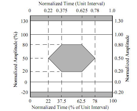
Output Eye Mask | Compliant with IEEE802.3 ah (class 1 laser safety) | Note (2) | ||||
Note (1): Measure at 2^7-1 NRZ PRBS pattern
Note (2): Transmitter eye mask definition, and eye mask diagram with at least 10% margin.
Specification of Receiver
Parameter | Symbol | Min. | Typ. | Max. | Unit | Note |
Input Optical Wavelength | λIN | 1500 | 1550 | 1600 | nm | GACC-3512-10D |
1260 | 1310 | 1360 | GACC-5312-10D | |||
Receiver Sensitivity | PIN | -19.5 | dBm | Note (1) | ||
Input Saturation Power (Overload) | PSAT | -3 | dBm | |||
Los Of Signal Assert | PA | -36 | dBm | |||
Los Of Signal De-assert | PD | -22 | dBm | Note (2) | ||
LOS Hysteresis | PA-PD | 0.5 | 2 | 6 | dB |
Note (1): Measured with Light source 1550nm(1310nm), ER=9dB; BER =<10^-12 @PRBS=2^7-1 NRZ
Note (2): When LOS de-asserted, the RX data+/- output is signal output.
Electrical Interface Characteristics
Parameter | Symbol | Min. | Typ. | Max. | Unit | Note | |
Transmitter | |||||||
Transmitter Disable Input-High | VDISH | 2 | Vcc+0.3 | V | |||
Transmitter Disable Input-Low | VDISL | 0 | 0.8 | V | |||
Transmitter Fault Input-High | VTxFH | 2 | Vcc+0.3 | V | |||
Transmitter Fault Input-Low | VTxFL | 0 | 0.8 | V | |||
Receiver | |||||||
LOSS Output Voltage-High | VLOSH | 2 | Vcc+0.3 | V | LVTTL | ||
LOSS Output Voltage-Low | VLOSL | 0 | 0.8 | V | |||
Digital Diagnostic Functions
GACC-3512/5312-10D transceivers support the 2-wire serial communication protocol as defined in the CSFP MSA. It is very closely related to the E2PROM defined in the GBIC standard, with the same electrical specifications.
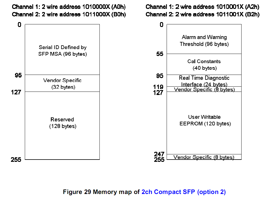
The standard CSFP serial ID provides access to identification information that describes the transceiver’s capabilities, standard interfaces, manufacturer, and other information.
Additionally, CSFP transceivers provide a unique enhanced digital diagnostic monitoring interface, which allows real-time access to device operating parameters such as transceiver temperature, laser bias current, transmitted optical power, received optical power and transceiver supply voltage. It also defines a sophisticated system of alarm and warning flags, which alerts end-users when particular operating parameters are outside of a factory set normal range.
The CSFP MSA defines a 256-byte memory map in E2PROM that is accessible over a 2-wire serial interface at the 8 bit address 1010000X (A0h) or 1011000X(B0h). The digital diagnostic monitoring interface makes use of the 8 bit address 1010001X (A2h) or 1011001X(B2h), so the originally defined serial ID memory map remains unchanged. The digital diagnostic memory is defined as follow:
The operating and diagnostics information is monitored and reported by a Digital Diagnostics Transceiver Controller (DDTC) inside the transceiver, which is accessed through a 2-wire serial interface. When the serial protocol is activated, the serial clock signal (SCL, Mod Def 1) is generated by the host. The positive edge clocks data into the SFP transceiver into those segments of the E2PROM that are not write-protected. The negative edge clocks data from the SFP transceiver. The serial data signal (SDA, Mod Def 2) is bi-directional for serial data transfer. The host uses SDA in conjunction with SCL to mark the start and end of serial protocol activation. The memories are organized as a series of 8-bit data words that can be addressed individually or sequentially.
Digital diagnostics for the GACC-3512/5312-10D are internally calibrated by default.
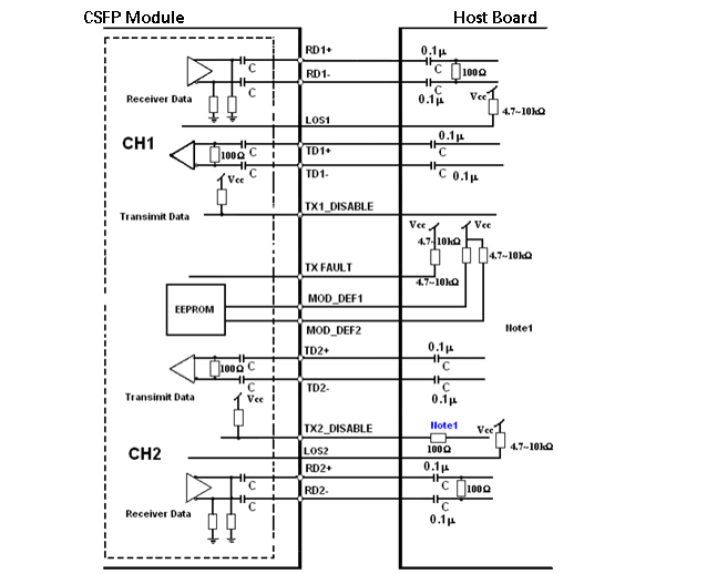
Recommend Circuit Diagram
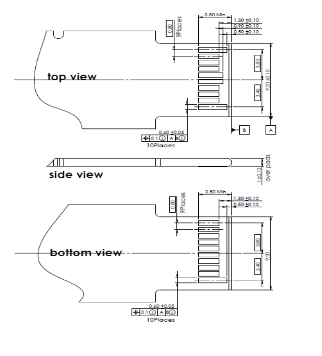
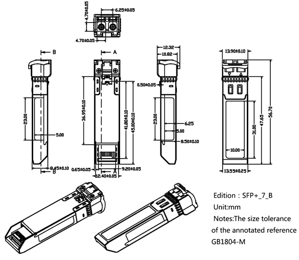
Outline Dimensions (mm)
Notice
Gigac reserves the right to make changes to or discontinue any optical link product or service identified in this publication, without notice, in order to improve design and/or performance. Applications that are described herein for any of the optical link products are for illustrative purposes only. Gigac makes no representation or warranty that such applications will be suitable for the specified use without further testing or modification.
Revision History
Version | Initiated | Reviewed | Revision History | Release Date |
A0 | Fei.Han | Sean.Lin | Initialization | 2020-10-15 |
A1 | Sean.Lin | Haiyuan.li | updated parameter | 2024-03-21 |