NGC(MIL-DTL-64266) Fiber Optic Connector-Aviation Connector
Sep - 11, 2025
Home > News > Company new > Silicon photonics integration breaks the power consumption bottleneck of intelligent computing centers: Gigac Technology's "cold" solution
With east-west traffic in intelligent computing centers surging, optical interconnect energy consumption has surpassed 30%, making heat dissipation a significant contributor to data center OPEX. Again
-- Gigac TechnologyWith east-west traffic in intelligent computing centers surging, optical interconnect energy consumption has surpassed 30%, making heat dissipation a significant contributor to data center OPEX. Against this backdrop, Chengdu Gigac Technology Co., Ltd., leveraging its decade of experience in industrial-grade optical module technology and focusing on silicon photonics integration, has achieved over 30% reduction in module power consumption compared to traditional solutions by integrating optoelectronic components such as lasers, modulators, and detectors onto a single silicon-based chip. This provides a new approach to cooling intelligent computing centers.
Silicon Photonics Integration and Dynamic Control
Traditional pluggable optical modules use discrete components, resulting in low electro-optical conversion efficiency and high signal loss. Gigac Technology has introduced wafer-level silicon photonics technology, integrating optical transmission, modulation, and reception functions on a single chip. By heterogeneously integrating lithium niobate thin films on a six-inch patterned SiN wafer, this reduces optical transmission losses by 40%. Combined with a 7nm DSP chip, this reduces typical power consumption from 12W to below 9W, saving millions of kWh annually in a single data center. The heat dissipation area is also reduced by 50%. Combined with microring resonator non-volatile tuning technology, this eliminates the need for temperature-controlled maintenance power consumption.
Based on this foundation, software algorithms are used to optimize dynamic power consumption. Leveraging patented CN110572216A technology, the module replaces traditional APC hardware circuitry with MCU software and a PID algorithm, enabling real-time adjustment of the laser bias current, improving optical power stability by 60% and reducing peripheral circuit power consumption by 15%. The modulator incorporates an MCU programmable architecture (patent CN202120298860.3), enabling coordinated top-modulation signals and APC control, enabling the module to automatically enter sub-photon power consumption mode (<0.05 photons/operation) under low load. The industrial-grade module features a built-in multi-stage step-down circuit and a temperature sensing algorithm to control power consumption fluctuations to within ±5% across the full temperature range of -40°C–85°C.
Reliability Design and Technological Evolution
To address the high-temperature demands of edge nodes in intelligent computing centers, Gigac Technology has infused its silicon photonic modules with industrial-grade expertise. The silicon photonic chip packaging leverages the electromagnetic shielding technology of patent CN120276099A and utilizes a composite material with a dynamically tuned dielectric constant, resulting in a 20dB improvement in electromagnetic interference suppression and a thermal conductivity exceeding 5W/mK. The plug-in optical module design eliminates optical fiber vibration loss. Combined with the vibration resistance of the silicon photonic chip, it achieves a bit error rate better than 10⁻¹² at 80°C. The metal housing is pre-installed with a microfluidic interface, and when connected to a cabinet-level liquid cooling system, power consumption remains below 16W at 50°C.
For the 1.6T era, CPO co-packaged optics are being deployed. By co-packaging the silicon photonics engine and ASIC chip on the same substrate, the electrical channel length is reduced from centimeters to millimeters, reducing signal loss by 70% and power consumption by another 30%. A hybrid integration solution using silicon photonics and thin-film lithium niobate enables a modulator drive voltage of only 1V, 80% lower than pure silicon solutions, supporting a baud rate of 200GBaud and laying the foundation for 3.2T CPO. The development of an integrated package using an aluminum nitride ceramic substrate and microchannel liquid cooling reduces thermal resistance to 0.15°C/W, addressing the hot issues associated with high CPO integration.
Industry Chain Collaboration and Effectiveness Verification
Gigac Technology is strengthening technology implementation through industry chain collaboration. Collaborating with research institutions on the "Universal Ion Knife" stripping technology, Gigac Technology has achieved a yield exceeding 90% for six-inch lithium niobate thin-film wafers. Leveraging the "Eastern Data West Computing" project, Gigac Technology is deploying a silicon photonics chip production line in Chengdu, leveraging the western region's low temperatures and green electricity resources to reduce production energy consumption. Gigac Technology also participated in the development of the "Data Center CPO Technology White Paper," promoting interface standardization to reduce integration costs.
Key Parameter Comparison: The table below compares the power consumption of optical modules using different technology paths.
| Technology Type | EER | Cooling Cost Ratio | Transmission Density | Temperature |
| Traditional Pluggable Modules | 3.5-4.2(pJ/bit) | 38% | 1.2Tbps/mm² | 0-70°C |
| Gigac Silicon Photonics Integrated Modules | 2.0~2.5(pJ/bit) | 22% | 3.8Tbps/mm² | -40°C~85°C |
| CPO (Under Development) | 0.8~1.2(pJ/bit) | <15% | 8.5Tbps/mm² | -40°C~105°C |
As intelligent computing centers enter the 200kW/cabinet era, the "performance per watt" of optical interconnects has become a core competitive advantage. Gigac Technology, using silicon photonics integration as its bow and software-defined arrows, is aiming for the high-power target:
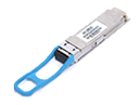
· Short-term: Leveraging 800G silicon photonics modules (power consumption <16W) to capture the East-West computing node market;
· Long-term: Through CPO + thin-film lithium niobate hybrid packaging, achieving the ultimate "optical in, copper out" replacement in the 3.2T era.
This technological evolution epitomizes the Chinese optical chip industry's shift from "following" to "defining"—when every joule of electricity is precisely converted into a stream of bits, the green genes of intelligent computing centers are nurtured and grown.
As a university professor put it, "The essence of silicon photonics integration is to allow photons to reach their destination in the most elegant way." Gigac Technology's practice embodies this elegance: using the dance of light on a silicon substrate to inject a breath of fresh air into the surging sea of computing power.
lf you have questions about our products, please feel free to contact us.
We will answer you as soon as possible.