


Products Description
Features
Single fiber bi-directional data links asymmetric TX 2488Mbps/RX1244Mbps application
1490nm continuous-mode DFB laser transmitter and 1310nm burst-mode APD-TIA receiver
Small Form Factor Pluggable package with SC/UPC Connector
Reset burst-mode receiver design support more than 15dB dynamic range
Single +3.3V power supply
Digital diagnostic monitoring interface
Digital burst RSSI function to monitor the input optical power level
LVPECL compatible data input/output interface
LVTTL transmitter disable control
LVTTL transmitter laser fault alarm
LVTTL receiver Signal Detect (SD) indication
Low EMI and excellent ESD protection
Class I laser safety standard IEC-60825 compliant
Operating case temperature:
Standard: 0℃~+70℃
Industrial: -40℃~+85℃
RoHS 2.0 compliance
Applications
Gigabit-capable Passive Optical Networks (GPON) B+/C+/C++/D/D1/D2/D3/D4/D5 20Km application
General
The GPON OLT Transceiver module is designed for Gigabit Ethernet Passive Optical Network(GPON)20km transmission. The module incorporates 1490nm continuous-mode transmitter and 1310nm burst-mode receiver. The transmitter section uses a 1490nm DFB laser and an integrated laser driver which is designed to be class-1 eye safe under any single fault. The laser driver includes APC and temperature compensation functions, which are used for keeping the launch optical power and extinction ratio constant over temperature and aging.
The receiver section uses an integrated APD and BM-preamplifier mounted together. The module has the function that indicates receiver burst-power-detect signal. The receiver includes digitalized burst mode optical power monitoring function, which converses any of a received ONU optical power directly in digital, with a Trigger input from system. When rising edge of Trigger detected, the DDM processor starts a burst optical power conversion, the digital result is available via DDM interface after Burst Optical Power Conversion Time. Trigger pulse width should be more than Burst Optical Power Conversion Holding Time. An integrated WDM coupler can distinguish 1310nm input light from 1490nm output light. The metallic package guarantees excellent EMI and EMC characteristics.
Order Information
Table 1-Order Information
Part Number | Data Rate (TX/RX) | Index level | PO (dBm) | Sens (dBm) | Interface | Temp. |
WGLS-4121-20xNote 1SxNote 2xNote 3 | 2.488/1.244Gbps | B+ | +1.5~+5 | ≤-28 | SC | C/I |
WGLS-4121-30xNote 1SxNote 2xNote 3 | 2.488/1.244Gbps | C+ | +3~+7 | ≤-30 | SC | C/I |
WGLS-4121-40xNote 1SxNote 2xNote 3 | 2.488/1.244Gbps | C++ | +4.5~+10 | ≤-31 | SC | C/I |
WGLS-4121-50xNote 1SxNote 2xNote 3 | 2.488/1.244Gbps | D | +6~+10 | ≤-33 | SC | C/I |
WGLS-4121-51xNote 1SxNote 2xNote 3 | 2.488/1.244Gbps | D1 | +7~+10 | ≤-33 | SC | C/I |
WGLS-4121-52xNote 1SxNote 2xNote 3 | 2.488/1.244Gbps | D2 | +8~+10 | ≤-33 | SC | C/I |
WGLS-4121-60xNote 1SxNote 2xNote 3 | 2.488/1.244Gbps | D3 | +9~+13 | ≤-33 | SC | C/I |
WGLS-4121-61xNote 1SxNote 2xNote 3 | 2.488/1.244Gbps | D4 | +10~+13 | ≤-33 | SC | C/I |
WGLS-4121-62xNote 1SxNote 2xNote 3 | 2.488/1.244Gbps | D5 | +11~+13 | ≤-33 | SC | C/I |
Note:
1. “x”=C : Operating case temperature Standard 0~70℃
“x”=I : Operating case temperature Industrial -40~85℃
2. Receiver Signal Detected
“x”=S:RX-SD (RX-SD=0:signal loss RX-SD=1:signal valid);
“x”=L:Rx-LOS (RX-LOS=0:signal valid RX-LOS=1:signal loss).
3. TX Power & Bias A/W Thresholds
“x”=1: TX Power A/W Thresholds 1LSB=0.1uW,TX Bias A/W Thresholds 1LSB=2uA
“x”=2: TX Power A/W Thresholds 1LSB=0.2uW,TX Bias A/W Thresholds 1LSB=4uA
Absolute Maximum Ratings
Table 2-Absolute Maximum Ratings
Parameter | Condition | Unit | Min. | Typ. | Max. |
Supply Voltage | V | -0.5 | - | 3.6 | |
Storage Temperature | Case Temperature | ℃ | -45 | - | +85 |
Relative Humidity, Storage | None Condensing | % | +5 | - | +95 |
Rx Total Optical Power | Damage Threshold | dBm | - | - | -8 |
Operating Environment
Table 3-Operating Environment
Parameter | Condition | Unit | Min. | Typ. | Max. |
Power Supply Voltage | V | 3.13 | 3.3 | 3.47 | |
Operating Case Temperature | Standard | ℃ | 0 | - | +70 |
Industrial | ℃ | -40 | - | +85 |
*Exceeding any one of these values may destroy the device immediately.
Electrical Characteristics
Table 4-Electrical Characteristics
Parameter | Symbol | Min | Type | Max | Units | Notes | |
Transmitter | |||||||
Differential Data Input Swing | Vin | 200 | - | 2400 | mVpp | 1 | |
Input Differential Impedance | Zin | 90 | 100 | 110 | ohm | ||
Tx_Disable | Disable | VD | 2.0 | - | VCC | V | |
Enable | VEN | GND | - | GND+0.8 | V | ||
TX_ Fault | Fault | VF | 2.0 | - | VCC | V | |
Normal | VNO | GND | - | GND+0.8 | V | ||
Receiver | |||||||
Differential Date Output Swing | Vout | 600 | - | 1500 | mVpp | 2 | |
Output Differential Impedance | Zout | 90 | 100 | 110 | ohm | ||
Signal Detect de-assert Time | TSDD | ns | - | - | 12.8 | 3 | |
Signal Detect assert Time | TSDA | ns | - | - | 50 | 4 | |
Signal Detect Voltage | High | VOH | 2.4 | - | VCC | V | |
Low | VOL | GND | - | GND+0.4 | V | ||
Note:
1. Internally AC coupled, input termination may be required for LVPECL/CML applications.
2. Internally DC coupled, LVPECL/CML differential output stage.
3. Refer to the Reset signal rising edge
4. Refer to the Reset signal falling edge.
Specifications
Table 5-Optical Characteristics
Parameter | Symbol | Units | Min. | Typ. | Max. | Notes |
Transmitter | ||||||
Data Rate | BR | Mbps | - | 2488 | - | |
Optical Center Wavelength | λC | nm | 1480 | 1490 | 1500 | |
Optical Spectrum Width (-20dB) | ∆λ | nm | - | - | 1 | |
Side Mode Suppression Ratio | SMSR | dB | 30 | - | ||
Power-OFF Transmitter Optical Power | dBm | - | - | -39 | 3 | |
Extinction Ratio | ER | dB | 8.2 | - | - | 4 |
Tolerance to Transmitter Incident Light | dB | -15 | - | - | ||
Transmitter and Dispersion Penalty | TDP | dB | - | - | 1 | |
Optical Waveform Diagram | ITU-T G.984.2 | 5 | ||||
Parameter | Symbol | Unit | Min | Typ. | Max | Notes |
Receiver | ||||||
Data Rate | BR | Mbps | - | 1244 | - | |
Operating Wavelength | λC | nm | 1260 | 1310 | 1360 | |
Saturation Optical Power | PSAT(B+) | dBm | -8 | - | - | 6 |
PSAT(C+,C++) | dBm | -12 | - | - | 6 | |
PSAT(D,D1,D2,D3,D4,D5) | dBm | -15 | - | - | 6 | |
Signal Detect Assert Level | SDA | dBm | - | - | -34 | 6 |
Signal Detect De-Assert Level | SDD | dBm | -45 | - | - | 6 |
Signal Detect Hysteresis | dBm | 0.5 | - | 6 | ||
Receiver Reflectance | dB | - | - | -12 | ||
Receiver Burst Mode Dynamic Range | dB | 15 | 7 | |||
Note:
1. BOL, Normal Temperature.
2. EOL, Over Temperature.
3. Launched into SMF
4. PRBS 2^23-1+72CID @2488Mbs
5. Figure 1
6. PRBS 2^23-1+72CID@1244Mbps BER≤10E-10.
7. Figure 2.
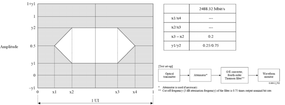
Figure 1 Transmitter Eye Mask Definitions and Test Procedure
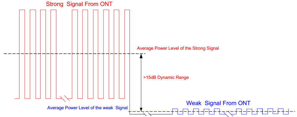
Figure 2 Burst Mode Receiver Dynamic Range in GPON System
Table 6-Digital RSSI Timing Specification
Parameter | Symbol | Unit | Min | Typ. | Max | Notes |
Guard time | TGUARD | bits | - | 32 | 1 | |
Reset width | TRESET | bits | - | 16 | 1 | |
Optical Signal During Time | TONT EN_DUR | ns | 500 | - | - | 2 |
RSSI Trigger Delay | TD | ns | 30 | - | 3000 | 3,4 |
RSSI Trigger width | TW | ns | 300 | - | TONTEN_DUR-TD | 4 |
I2C Access Prohibited Time | us | 500 | - | |||
Measurement Accuracy of received burst optical power, range from -10dBm to -30dBm | dB | -3 | - | +3 |
Note:
1. Figure 3.
2. For RSSI Measurement, Figure4.
3. Refer to first bit of the preamble.
4. Figure 4.
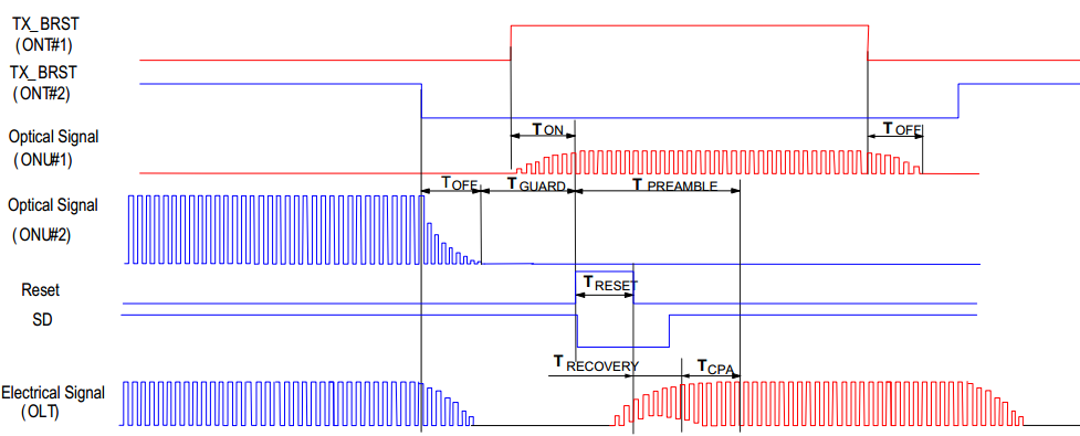
Figure 3 Burst Receiver Timing Sequence
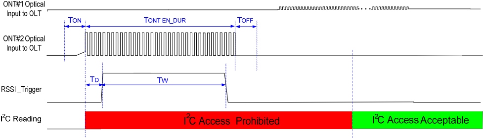
Figure 4 RSSI Timing Sequence
Digital Diagnostic Memory Map
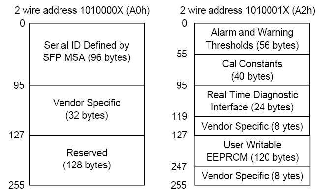
Figure 5 Memory map
Pin arrangement
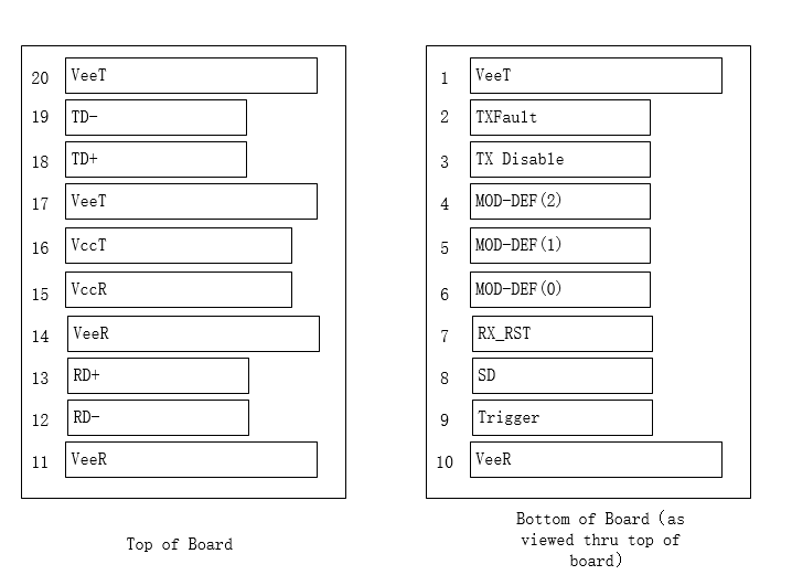
Figure 6 Pin Views
Table 7-Connector Pin Assignment
Pin | Name | Description | Notes |
1 | VeeT | Transmitter Ground | |
2 | TXFault | Transmitter Fault Indication | High: abnormal; Low: normal |
3 | TX Disable | Transmitter Disable | High: transmitter disable; Low: transmitter enable |
4 | MOD-DEF(2) | Module Definition 2 | I2C data, SDA ,The data line of two wire serial interface |
5 | MOD-DEF(1) | Module Definition 1 | I2C clock, SCL ,The clock line of two wire serial interface |
6 | MOD-DEF(0) | Module Definition 0 | Connected to Ground in the transceiver |
7 | RX_RST | Receiver Reset | Active High |
8 | SD | Signal Detect | High: signal detected; Low: loss of signal |
9 | Trigger | RSSI Trigger for Transceiver A/D Conversion | High: enable RSSI A/D conversion |
10 | VeeR | Receiver Ground | |
11 | VeeR | Receiver Ground | |
12 | RD- | Inverse Received Data out | LVPECL logic output, DC coupled |
13 | RD+ | Received Data out | LVPECL logic output, DC coupled |
14 | VeeR | Receiver Ground | |
15 | VccR | Receiver Power —— +3.3V±5% | |
16 | VccT | Transmitter Power —— +3.3 V±5% | |
17 | VeeT | Transmitter Ground | |
18 | TD+ | Transmitter Data In | LVPECL logic input, AC coupled, internally 100 ohms differential termination |
19 | TD- | Inverse Transmitter Data In . | LVPECL logic input, AC coupled, internally 100 ohms differential termination |
20 | VeeT | Transmitter Ground |
Block Diagram
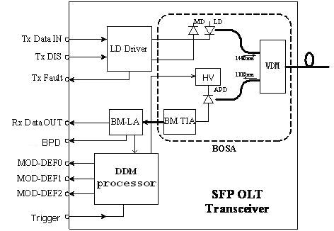
Figure 7 Block Diagram
Typical Application Circuit
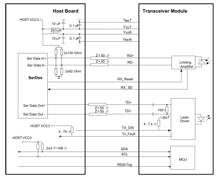
Figure 8 Typical Application Circuit
Mechanical Information
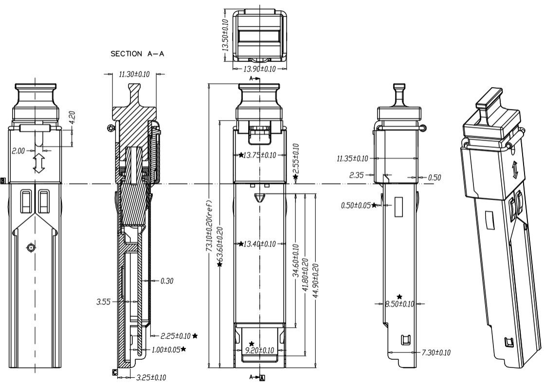
Figure 9 Mechanical Information
Regulatory Information
Table 8-List of Regulatory/Compliance
Feature | Standard | Performance |
Electrostatic Discharge (ESD) to the Electrical Pins | MIL-STD-883H Method 3015.8 | Based on HBM |
IEC61000-4-2 | 8kV Contact Discharge 15kV Air Discharge | |
Electrostatic Discharge to the enclosure | EN 55024:1998+A1+A2 IEC-61000-4-2 GR-1089-CORE | Compatible with standards |
Electromagnetic Interference (EMI) | FCC Part 15 Class B EN55022:2006 CISPR 22B :2006 VCCI Class B | Compatible with standards Noise frequency range: 30MHz to 6GHz. Good system EMI design practice required to achieve Class B margins. System margins are dependent on customer host board and chassis design. |
Immunity | EN 55024:1998+A1+A2 IEC 61000-4-3 | Compatible with standards. 1KHz sine-wave, 80% AM, from 80MHz to 1GHz. No effect on transmitter/receiver performance is detectable between these limits. |
Laser Eye Safety | FDA 21CFR 1040.10 and 1040.11 EN (IEC) 60825-1:2007 EN (IEC) 60825-2:2004+A1 | CDRH compliant and Class I laser product. |
RoHS 2.0 | 2011/65/EU | Compliant with standards |
Notice
Gigac reserves the right to make changes to or discontinue any optical link product or service identified in this publication, without notice, in order to improve design and/or performance. Applications that are described herein for any of the optical link products are for illustrative purposes only. Gigac makes no representation or warranty that such applications will be suitable for the specified use without further testing or modification.
Revision History
Version | Initiated | Reviewed | Revision History | Release Date |
A0 | Fei.Han | Smith.Xu | Initialization | 2018-07-16 |
A1 | Fei.Han | Sean.Lin | PX30 Index level series Added | 2022-09-01 |
Contact
Add: Area 3-502, Haolang technology Park,
NO.2666, Konggang Four Road, Shuangliu district, 610207 Chengdu, China
Tel: (+86) 028-85124518
Fax: (+86) 028-85154518
Postal: 610207
E-mail: sales@gigac.com
Website: http://www.gigac.com
Our factory
 and combiner unit (OMU)")
Wavelength Divisio···

Detailed Explanati···

The Working Princi···

The Key Difference···
Hot Tags:
R&D laboratory
Gigac has introduced numerous precision testing equipment, such as Ixia XGS12, Ixia WaveTest 93, Anritsu, Fujikura, Fluke, JDSU, Agilent, EXFO, DATA-PIXEL, etc., for product development testing and validation.At present, there are over 100 professional engineers, of which 50% are senior engineers. Through standardized testing processes and in line with international professional testing standards, we provide testing in various aspects such as product appearance, performance, compatibility, and solution scenarios to meet the diverse testing needs of global customers.
Numerous research and development achievements
Gigac adopts a research and development model that combines independent research and joint development, and has achieved outstanding results in industrial design and product software and hardware research and development.As data centers continue to expand and grow, a well planned cabling infrastructure is crucial. Without flexible cabling plans that can easily adapt to common moves, additions, and changes, your network growth will be limited. The Gigac series high-density data center cabling solutions can simplify deployment, enabling up to 144 LC fibers in 1U, and enabling flexible expansion and rapid upgrades with increasing business traffic demands.
Gigac Test Center
Gain a comprehensive understanding of Gigac's optical modules, fiber optic jumpers, and enterprise network testing center. We have a comprehensive testing plan, professional testing equipment, and standard testing procedures. We regularly test optical modules, cables, switches, and other products to ensure that we provide high-quality products to our partners.