

1. Background of the problem
During the testing process of the 10G BIDI project, it was found that the alarm would be delayed or even not triggered. It was further discovered that the module alarm (LOS-A) and de alarm (LOS-D) were normal when not mounted, and the sensitivity (SEN) would also increase. However, after mounting, some modules had delayed alarms and de alarms, and some modules even did not alarm, resulting in a general decrease in sensitivity.
2. Problem analysis and positioning
The three indicators of the receiving end of the module before and after shell installation show abnormalities, and it is preliminarily suspected that the receiving end is caused by crosstalk from the transmitting end. To verify this hypothesis, we powered on the module with the shell and manually turned off the transmission through software. The three indicators of the receiving end all showed significant improvement, which was basically consistent with the indicators when the shell was not installed.
By adjusting the BIAS and MOD current output of the driver chip (ONET1151) separately, it can be determined whether the crosstalk affecting the receiving end indicators is optical or electrical! The 10G BIDI project adopts AC coupled output, and the only contribution to the emitted optical power is the BIAS current. If only three indicators of the BIAS current receiving end are changed, there will be improvement, and it can be determined that it is optical crosstalk; If only MOD current affects it, it can be determined that it is electrical crosstalk. Therefore, we conducted the following experiments:
1. When keeping the output BIAS current constant and changing the magnitude of the MOD current, the ER at the transmitting end changes from 0dB to 4.2dB, and all three indicators show significant changes;
2. Keep the MOD current constant, and adjust the BIAS current size to ensure that the three indicators remain basically unchanged;
From this experiment, we can determine that the interference of the electrical signal at the transmitting end affects the performance of the receiving end.
Through in-depth analysis of the causes of electrical crosstalk, it is not difficult to find from the Pin Connection of component 1 in Figure 1 and Figure 2 that the PD connection VCC (Source type on ONET1151L), PD+(CASE pin) is connected to ground, so the entire shell of the module is grounded. On our module, both the transmitting and receiving FPCs are attached to the surface shell, especially the transmitting FPC is attached to the surface shell, as shown in Figures 3A and 3B. Therefore, the differential lines on the transmitting and receiving FPCs are tightly attached to the ground. Therefore, we preliminarily conclude that this is because the signal from the transmitting end is coupled to the receiving end through the surface shell. In addition, the degree to which the flexplate and the surface shell are attached will also affect the indicators of the receiving end to varying degrees.
![af85cc151d10c9aa8304aa67a4487a8d[1].png](/static/upload/image/20240227/1709002569185874.png)
Figure 1 TOP VIEW
![79b7f1b050d139301dceed7ccf220fd0[1].png](/static/upload/image/20240227/1709002683368427.png)
Figure 2 Schematic diagram of 10G BIDI BOSA transmitter
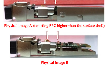
Figure 3
3. Validation and data analysis
To verify whether the interference of electrical signals at the transmitting end affects the performance of the receiving end, we conducted two types of comparative experiments as follows.
1. Place adhesive tape or high-temperature adhesive tape at the position where the surface shell comes into contact with the emitting FPC. Experimental results have shown that the isolation of the adhesive tape is better than that of high-temperature adhesive tape. The indicator parameters of the module with adhesive tape are basically the same as those of the module when the emission is turned off, without considering measurement errors. Here, only data statistics were conducted on the module before and after applying high-temperature adhesive tape. The specific data are as follows (at room temperature and low temperature):
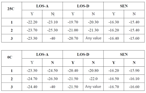
Note: Y represents tape applied, N represents no tape applied
From the comparison of the above data, it is not difficult to find that under normal temperature and low temperature conditions, both the alarm and de alarm indicators on the module without adhesive tape will be delayed, and the sensitivity will decrease. This is because the receiving end is affected by the signal interference from the transmitting end, which requires smaller downlink light to alarm while keeping the alarm threshold unchanged. The sensitivity will also be severely reduced due to the crosstalk from the transmitting end, After applying adhesive tape to the module, the isolation effect on the transmitted signal is very obvious. The signal from the transmitting end will not be coupled to the receiving end through the surface shell, and the sensitivity indicators will not be affected.
2. Considering the issue of production feasibility in the future, we will weld the FPC surface by connecting one side of the differential line on the FPC to the TOP surface of the PCB, as shown in Figures 4A and 4B. We will also cut off the PD pad on the transmitting flexplate, adjust the module to the same PO and ER as in the closed loop under open-loop conditions, and record the three indicator data of the receiving end under both conditions. The specific data is shown below (only one module has been experimentally compared at room temperature):
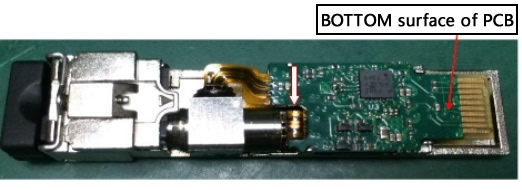
Figure 4A: Differential line of FPC emission on the same side as BOTTOM surface (before exchange)
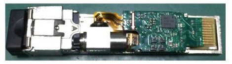
Figure 4B: The differential line of FPC emission is on the same side as the TOP surface (after exchange)
It is not difficult to find from this set of data that when there is no cover before switching, that is, when there is no crosstalk, the three indicators of alarm, alarm removal, and sensitivity at the receiving end are the best. When the differential line of the transmitting FPC is on the same side as the BOTTOM surface (before switching), the receiving end is greatly affected by crosstalk at the transmitting end, with a sensitivity decrease of about 0.8dBm, and both alarm and alarm removal are also affected; When the differential line of the transmitting FPC is on the same side as the TOP surface (after exchange), the sensitivity of the receiving end only decreases by 0.3dBm, which is about 0.5dBm higher than before exchange. The alarm and de alarm are also improved to a certain extent.
From the above analysis, it can be determined that after welding the transmitting FPC, the crosstalk at the receiving end will be greatly reduced. If the differential line of the receiving FPC is also placed on the same side as the TOP surface, the crosstalk at the receiving end will be further improved or even non-existent. However, due to the symmetrical placement of VCC and RSSI pads in the receiving FPC, the experiment of welding the receiving FPC is not easy to carry out; This experiment will be confirmed after redesigning the FPC in the future to ensure that crosstalk is minimized.
4. Conclusion
In the 10G BIDI project, the indicators of the receiving end (alarm LOS A, de alarm LOS D, sensitivity SEN) were not ideal. After experimental verification and analysis, it was confirmed that the signal from the transmitting end was coupled to the receiving end through the surface shell, causing the three indicators of the receiving end to be affected. Two methods, namely sticking tape on the surface shell and changing the surface of the transmitting flexible plate for welding, were used to reduce crosstalk and greatly improve the indicators. In the future, it is hoped to redesign the flexible plate, The method of placing the differential lines in the transmitting and receiving flexible plates on the same side as the TOP surface of the PCB further reduces crosstalk.