

Overview of EPON OLT Optical Module
When the OLT optical module is working, the downlink uses broadcasting to continuously transmit data streams, and each ONU can receive the OLT signal, regardless of whether the signal is for itself. Therefore, the transmission of the OLT in the downlink direction is continuous, and the reception of the ONU is also continuous. Due to the TDMA multiplexing method used in the uplink, each ONU can only send data during the allowed time period. Therefore, in the uplink direction, the transmission of ONU is burst, and the reception of OLT requires burst operation. Therefore, the reception of OLT optical module has strict timing requirements.
The structural diagram of EPON OLT is as follows: in the emission part, a 1490nm DFB laser is driven by NT25L90; The receiving part uses a limiting amplifier SY88903ALK to convert the voltage signal amplified by TIA into a voltage level; The control circuit part uses a C8051F392 microcontroller to complete module monitoring and reporting, as well as module work control; In the boost section, the MP3217 boost chip is used to provide reverse high-voltage bias to the APD.
![afede13ee70adc60b6cd8be8930b0705[1].png](/static/upload/image/20240227/1708997232403108.png)
Figure 1: EPON OLT Structure Block Diagram
EPON OLT receiving circuit and control timing
1.EPON OLT receiving circuit
The schematic diagram of the receiving end is shown in Figure 2. The high voltage of APD is provided by the boost chip MP3217 times the voltage. After passing through the DS3920 mirror tube, the mirror voltage output MIROUT pin is connected to the APD tube core to provide current monitoring IMIROUT. The mirror current output pin MIR, and the output current IMIR=1/5 IMIROUT. EPON OLT requires an external TRRIGER to control the sampling of burst received signals. Here, TS5A4594DCK analog switch is used for external TRRIGER control. Receive signal strength monitoring RSSI signals, which are amplified and processed by MAX4232AKA operational amplifier before being sent to MCU for acquisition and processing. The MCU triggers with the rising edge of the TRIGGER signal, detects the TRIGGER signal, and after a delay of 1 us, continuously collects 4 RSSI AD values to take the average. MCU provides a stable reference voltage VREF to maintain the voltage stability of APD.
![ca7836eda820c5688cc08717b5b17958[1].png](/static/upload/image/20240227/1708997492154463.png)
Figure 2: EPON OLT receiver schematic diagram
2. EPON OLT receiving timing
EPON OLT has high requirements for timing, and timing control is shown in Figures 3 and 4.
a. The minimum packet length of the test light ONU1 is set to 1us, the packet interval is set to 512bits, and the leading 512bits.
b. The minimum packet length of the interference light ONU2 is set to 1us, the packet interval is set to 512bits, and the leading 512bits.
c. Trigger with a delay of 500ns and a width not exceeding 600ns.
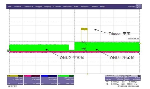
Figure 3: EPON OLT Receiving timing
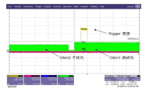
Figure 4: EPON OLT Receiving optical signal timing
EPON OLT RSSI problem analysis
The optical power reception range of EPON OLT is -6dBm to -30dBm, and RSSI reporting needs to be controlled within ± 2dB. During prototype debugging, it was found that the RSSI report of the module exceeded 2dB at the point of receiving small light of -30dBm, and there was a 1-2 value fluctuation in the sampled AD value.
1. The reference output voltage VREF of the MCU is 2.40V without any jumping, and the output voltage of the VAPD pin is 48.5V without any jumping. Disconnect the boost circuit on the OLT module and use the boost circuit of other optical modules to provide high voltage. It was found that the RSSI AD value was also jumping. Replacing the TS5A4594DCK analog switch did not improve the jumping of the RSSI AD value. Through the above detection, the impact of boost circuit noise on RSSI can be ruled out.
2. In hardware circuit diagram 2, the sampling and holding circuit values R50=6K, C47=22PF, RSSI sampling 7 points and corresponding AD fitting curves are shown in Figure 5. It can be observed that there are only a few AD values between -30dBm and -26dBm in the AD variation of Xiaoguang, which can lead to a significant deviation in the RSSI report of 1-2 AD values collected by the MCU. Increasing the sampling resistor R50 will increase the decrease time of the sampling level, and there is a contradiction between the two. The MCU AD is a 10-bit ADC, and replacing it with a high-precision 14-bit ADC MCU requires a new solution. At this point, the problem has arisen. How can we increase the AD value collected by RSSI without changing the plan?
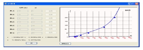
Figure 5: RSSI Fit curve
Under the unchanged MCU scheme, in order to amplify the acquisition AD value of RSSI in the small light section, a two-stage RSSI signal amplification RSSI gain variable circuit is proposed, as shown in Figure 6. Add an analog switch between the input pins of the operational amplifier, and when receiving small light, the analog switch will open to use a large amplification factor for the RSSI signal. When receiving high light, the analog switch is turned on and a small amplification factor is applied to the RSSI signal. This ensures that the AD value collected by low light is amplified, and the AD value collected by high light will not overflow. The RSSIAPD calibration fitting curve is shown in Figure 7. By verifying that the circuit can effectively improve the problem of RSSI AD jumping, RSSI reporting can be controlled within ± 2dB.
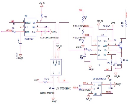
Figure 6: RSSI Gain variable circuit
![14eb2aa0e682746ee9da6cc02791a09c[1].png](/static/upload/image/20240227/1708998709110786.png)
Figure 7 RSSI Small Light and Large Light Fitting Curve
summary
The EPON OLT receiver requires high timing requirements, and in order to achieve high-precision RSSI reporting, it is necessary to control the high voltage noise of the power supply, analog switch noise, and layout RSSI wiring well. This scheme only has 10 ADC values in MCU, and the use of gain variable RSSI amplification circuit effectively solves the problem of insufficient accuracy in AD acquisition and reporting. At the same time, in the LYOUT wiring, it is necessary to minimize the interference of power supply noise, analog switch noise, high-speed signal lines TX/RX, and other signal lines on RSSI in order to improve the reporting accuracy of RSSI.